Showing posts with label PCB Assembly from India. Show all posts

Thursday, 13 May 2021

Printed Circuit Boards _ What & Why - Miracle Electronics

Printed Circuit Boards (or PCBs) are seen in almost every electronic device – that small green board with tiny black and golden components and connections. These tiny boards are capable of supplying electrical signals by connecting all the mounted electronic components together. 

There are a variety of PCBs available in the market, which can be selected depending upon the application it needs to be used in, and the purpose it needs to serve. Some of the most common PCBs seen are single-sided, double-sided , through-hole, and surface-mount. Let’s take a look at the types of PCBs and their applications below.

Types of PCBs

Single-sided PCBs

A single-sided PCB is the most basic type, which consists of a flat sheet of insulating material and a layer of copper foil laminated to the substrate. The copper is etched to divide it into separate conducting lines called traces. Then, there are all sorts of connections and electromagnetic shielding made possible with the help of insulated wires. The copper layer is finally coated to reduce the chances of shorts and prevent it from corrosion.

Double-sided PCBs

These PCBs are just like single-sided boards, but with copper layers and componentson both sides of the substrate layer , which allows the traces to cross over each other. This results in high-density complex circuits that are more difficult to produce. Double-sided PCBs can have their components connected using two technologies – through hole and surface mount. But, both these technologies come with their own benefits and limitations.

Through-hole PCBs

This is the most basic technology that has been used since initial times to produce PCBs, wherein the electronic components are mounted by leads inserted through holes on one side of the board, and soldered onto the copper traces on the other side. The leads are bent at 90 degrees to horizontally install the through-hole parts with two axial leads, inserted into the board, soldered, and trimmed off at the ends. The through-hole technology requires many holes to be drilled, limiting the available routing area for signal traces.

Surface-mount PCBs

Surface-mount technology  came after the through-hole technology to enable mounting of very small-sized components on the board, with small metal tabs or end caps that can be soldered directly onto the PCB surface, instead of wire leads passing through holes. With this technology, it became possible to mount components on both sides of the board easily; thus allowing very small PCB assemblies with much higher circuit densities. The technology is also automated, which reduces time and costs related to manual labour, thus increasing production rates.

Applications of PCBs

Electronic devices – PCBs are highly used in electronic devices, providing channels and pathways for electricity and signals to follow, thus allowing functioning of the device.

Computers – PCBs are very popularly seen in motherboards of computers, which makes complex functions possible too.

Medical devices – PCBs can help in the medical industry by performing a variety of functions like diagnosing, monitoring, and treatment. For instance, PCBs are used in the medical field in equipment like medical imaging systems, monitors, and infusion pumps. However, the PCBs to be used in medical devices should strictly comply to stringent standards for sanitation and functionality.

Automotive components – Automotive components need to withstand extreme temperatures and vibrations; and with the advancement of technologies, PCBs are not limited to windshield wipers and headlight switches only; rather they are also used in many other automotive components like control systems, stereo systems, navigation systems, and sensors.

Aerospace and military components – PCBs are also used in the most critical applications like aerospace and military. In the aerospace industry, PCBs are used in planes, satellites, space shuttles, and radio communication systems. And, in the military industry, PCBs are used in communication equipment, control systems in military vehicles, firearms, and more.

No matter what the application, you can always get the most appropriate PCB assembly for your equipment. And, when you’re looking for perfect products, you can always opt for Miracle Electronics’ customized solutions to get seamless PCB assembly manufacturing from India.


Tuesday, 27 April 2021

Should You Use Filled Or Untreated Vias For Your PCB - Miracle Electronics

Most manufacturers are opting for the surface mount technology for building PCBs, rather than the through hole technology, so as to allocate lesser space on the board, making them smaller and easier to install. But, with the rising use of surface mount technology components, more vias are being used too. Vias are holes for electrically connecting stacked pads on different circuit layers. 

While all vias essentially perform this same function, there can be different types of vias, depending upon their appearance on the PCB surface, namely through vias, blind vias, and buried vias.

Treating the vias

In order to improve the thermal performance of the PCB, there can also be done some additional treatments on the vias, such as filling, covering, capping, plugging, or tenting. Such treatments can help eliminate several assembly issues like shorting between component pads, or wicking down of the solder through the hole of a via. It can also eliminate expensive troubleshooting and reworking.

Filling – This treatment fills a regular or encroached via with non-conductive epoxy paste. These filles vias have the solder mask stopping short of the pad by a few mils, making it a good compromise for medium-density PCBs, as the presence of the solder mask reduces the likelihood of the solder bridging between the via and neighbouring pad.

Plugging – This treatment plugs one or both ends of the via with a non-conductive epoxy paste to prevent solder flow-through or wicking during soldering. But, in order to allow the epoxy to plug the hole effectively, the diameter of the via should be limited to a maximum of 20 mils.

Tenting – This treatment covers both pads at the end of the hole with a non-conductive solder mask, effectively sealing the openings. A dry film with a 4-mil thickness is adequate for covering even large holes effectively, without breaking down much. But today, manufacturers are opting out of the traditional dry film, and choosing modern LPI solder mask instead, which is only one-tenth the thickness of dry films.

Advantages of filled vias

Filling the vias can have several advantages over untreated ones, some of the benefits being high routing density, better conductivity (both thermal and electrical), and EMI reduction. Being very small in size, micro-vias allow high routing density on the PCB, allowing substantial reduction in the overall PCB size, and lowering the number of layers. All of this ultimately reduces the cost of the PCB. With a smaller size, there is also reduction in the distance between the components, which in turn reduces the overall resistance of the tracks, resulting in better electrical conductivity. This high conductivity in turn helps to lower the EMI reduction. Hence, filled micro-vias are particularly helpful for conducting a large amount of heat away from a hot component. The metallic nature of the filling wicks heat naturally away from the chip to the other side of the board for further dissipation by a heat sink.

If you want to take advantage of such filled micro-vias, you can always get in touch with Miracle Electronics to get your preferred customized PCB assembly from India. Get in touch and explain all your requirements and purposes, and you’ll get the most apt PCB assembly for your application, reliable and safe.


Tuesday, 30 March 2021

Why Approach A PCB Manufacturer For Box Build Manufacturing - Miracle Electronics

The PCB is a very tiny, yet most important piece of equipment, that makes every electronic device on the earth function as expected. And, to make this very tiny piece, it takes a lot of time and effort. The board has to be manufactured, the cables and harnesses built, and different sub-assemblies connected together to make one complete system. It may take hundreds, at times thousands, of tiny components to bring together one single board, which may make it very overwhelming for designers to form the perfect picture. But, there are some experts who can do the job just right; someone like Miracle Electronics, who has a skilled engineering team and facilities equipped with the latest technologies to ensure optimal and cost-effective production of even the most complicated and dense PCB assembly from India.

At Miracle Electronics, you can have the best quality PCB assemblies built using standardized procedures that translate unique customer requirements into production, every piece thoroughly tested for consistent quality performance; no matter what the size of the project, whether low, medium, high-mix, or high. Furthermore, they are also skilled at offering box builds, a complete package for innovative products, offering designs and finishing services for surface mount, through hole assemblies, cable manufacturing, panel wiring, and complete cabinet assemblies, with the help of dedicated lean manufacturing techniques in every operation. Why we say this is because outsourcing a box build assembly  to a PCB manufacturer can definitely help you in many ways, three most advantageous benefits mentioned below.

Hassles are reduced

Building a box build requires a lot of equipment like PCBs, cable assemblies, power supplies, control panels, and more. This means, if you want to take up the task on your own, you need to be associated with multiple vendors who can provide you with such different stuff. But, working with multiple vendors is a lot of hassle. It requires strong coordination and effective communication to manage everything, because one wrong vendor can result in an unlikely outcome. On the other hand, if you put the task on the shoulders of a reputed PCB and box build assembly manufacturer, they’ll make sure that the final circuit board fits in all the interconnecting wires and cables, working together with the other components.

Unnecessary overheads are eliminated

Having multiple vendors not only adds hassles and errors to the process, but it also increases the overhead costs. Passing on the equipment from one vendor to another, procuring the same at every step, and delivering it to another involves lots of time wastage, as well as additional expenses. Working with a single specialist can eliminate the expenses involved with operating and procuring the equipment from each vendor; thus making it easier and cost-effective, with no time delay.

Performance is guaranteed

The performance of a box build depends upon how well the components fit and work together. There are a variety of different components that needs to be designed and assembled in a box build to work together. And, a plan in place is very essential for the same. Different vendors handling different aspects of the process could cause hindrance in the plan. One wrong connection or component could result in an ineffective or faulty performance. The best way to eliminate such errors is by having one professional handle the entire task, from the beginning till the end. There will be no planning and communication issues if one specialist handles the task.

To conclude, teaming up with a professional PCB manufacturer who knows the A-Z of box build manufacturing is a wise decision. You could have your PCB assembly from India, cable assemblies, and every other component manufactured and connected effectively with one single specialist; and get the anticipated outcomes!

Monday, 22 March 2021

What Causes PCB Warpage & How To Avoid It - Miracle Electronics

Imagine, you receive a PCB package, but when you place it onto your application device, you realize that it doesn’t fit into the flat space available! Can you envisage how annoying and bothersome that may be! The reason behind such a scenario is board warping, the unintended change in the geometry of a PCB. A warped PCB is thus an altered PCB, regardless of the shape it forms into, such as bow, twist, etc. In short, a warped PCB is one that does not sit accurately on a flat surface.

What causes PCB warpage?

There are several reasons that could cause PCB warpage, but there are two specific causes – one of them could be layout-related, while the other could be process-related. If the PCB is warped before the beginning of the assembly process, the problem lies between the layout and fabrication. But, if the PCB was flat earlier, and warped after assembly, then the problem lies between the fabrication and assembly.

Design issues causing the warpage – There could be certain design issues that may contribute to PCB warpage, which need to be first and foremost eliminated, before moving onto the fabrication or assembly process. And, in order to eliminate them, you first need to know the main design contributors; some of them being odd shapes, large cut-outs, a thin board, grouping together of heavy components, and uneven copper pour.

Assembly issues causing the warpage – If polyimide or FR-4 is used to build a PCB, and a stack of such bare boards are stored for some time before assembling, they may absorb moisture from the environment, to eliminate which it is customary to bake them for at least 3 hours at 80-150°C first, and then cool them to room temperature before assembling.

Another reason for warpage in large boards may be related to the orientation as the boards enter the reflow oven. In order to prevent uneven heating between the edge of the PCB and the middle, the larger dimension must be placed parallel to the conveyor of the oven.

Small PCBs are generally grouped together to form panels for more efficient assembling, after which they are separated manually into individual PCBs. The separation takes place by either breaking them away or through V-scoring. In the process of breaking away, most of the material between the smaller PCBs is cut away, leaving them joined by only small lands; and if the panelization is large, the cut-outs could lead to warping. On the other hand, V-scoring is where a V-shaped groove forms the separation line, instead of removing a part of the PCB, which prevents warping of the panel during assembly, while making it easier to separate the boards.

How to prevent PCB warpage?

  • Storing the PCBs properly before the assembly process is crucial in preventing warpage. Standing them on their edge cannot guarantee that they will be vertical all the while. Moreover, the combined weight of the PCBs will ultimately cause a camber. It is thus important that the PCBs are stored properly, and horizontally on a flat surface.
  • PCBs should be stored in an area where the temperature and humidity is under control, because it is usual for PCBs to absorb moisture from the surroundings. And, where it is impractical to control the environment, desiccants can be used to control the moisture.
  • Just like PCB fabricators use heat to form multi-layered boards , re-application of heat to warped bare boards can help straighten them as well. But, this may require heavy-pressing the boards between heated smooth steel plates for 3-6 hours and baking the PCBs 2-3 times.

In order to prevent such warpage in your PCBs, you need to ensure that you get your PCB assembly from India from an experienced manufacture, who knows how to take care of every process involved in storing and manufacturing the PCBs well, such that every PCB is built successfully and effectively.

Friday, 22 January 2021

What Makes PCB Manufacturing So Precise - Miracle Electronics

PCB assemblies are so dense, so complicated, filled with so many tiny elements connected together, yet so precise! Have you ever wondered how something so tiny and complicated can be so precise? One of the major reasons for the precision is the latest technology used in manufacturing PCBs today. While earlier, PCB making was a manual process, over the years, the PCB manufacturing process has significantly changed, thanks to the latest technological innovations that have allowed PCB manufacturers to innovate accurately and skilfully. Here’s how a prototype PCB assembly from India is made  with such skill and accuracy.


Pre-manufacturing – Planning


Before a PCB prototype is begun for manufacturing, there is a lot of planning done, considering countless aspects. First and foremost, the PCB manufacturer will look over the design and Gerber files. Then, step-by-step instructions will be laid out for fabrication, which will be reviewed by an engineer, who will then convert these plans into a data format that will help engineer the board. Any issues will also be checked for with formatting or cleaning up. Based on this data, the final board will be created.

Manufacturing


Step 1 – Plotting


Once inspected and finalized, a panel array is then chosen for the best fit, after which photo plotting begins. This is the first step of the production process. A laser is used to plot the patterns, silk screens, and other primary images that are required on the PCB.


Step 2 – Lamination


In the case of multi-layered PCBs, the multiple layers need to be fused together, which can be attained with the help of lamination, that is done using heat and pressure.


Step 3 – Drilling


Once heat and pressure laminates the layers together, expert drilling systems are used, programmed to drill holes into the board, accurately and precisely. This drilling program ensures that there is no human error while manufacturing the PCB.


Step 4 – Copper Deposition and Plating


The copper layer of the PCB, which is deposited through electrolysis, is an important part of the PCB, the conductive property essential to the functionality of the PCB prototype. PCBs generally become conductive after electroplating, which is where the copper is plated via a plating bath. These copper tracks prove to be conductive tracks that connect two points within the circuit board.


Post-manufacturing – Testing


After the prototype is built, it is thoroughly tested in every way to identify any mistakes or flaws that may lead to errors or unexpected end results. Identifying these mistakes in the prototype can help correct them right there so that the rest of the manufactured products are not flawed, thus saving on costs and time. Once the prototype is confirmed to be perfect, the remaining lot is manufactured.


You can see how the latest technologies used bring such precision to PCBs. For such a precise and accurate PCB assembly from India, you can get in touch with Miracle Electronics, the leading PCB assembly manufacturer in the country, who is an expert in building PCBs of all kinds and sizes in world-class manufacturing environments to provide scalable, high-quality, and low-cost PCB assemblies to totally satisfy customers!


Thursday, 21 January 2021

Fiducial Markers – What They Mean For A PCB - Miracle Electronics

With PCBs being vital components of almost every electronic and electrical device today, it is important to take care of every detailing when designing a PCB. One way to get PCB designing right is by adding reference points to the design, which helps to keep the orientation right. Fiducial markers can help to provide such reference points for imaging systems.

What are fiducial markers?

The term “fiducial” means a fixed-point basis of reference; its purpose being to compare. Fiducial markers are surface marks that designers use as directional measures in indexing systems. These markers work as alignment marks in indexing systems of electronic assembly industries that use automation, helping to orient the PCBs in the right skews and directions. They allow the vision system to insert components precisely on the circuits. Fiducial PCB markers thus prove to be a vital aspect of the entire automated process. These fiducial markers consist of three parts – a solid copper ring on the top or bottom of the copper layer, the circle in the solder mark which is the target that needs to be aligned, and the option text label on the side.

The three benchmarks of a fiducial PCB

First datum – The first datum, depicted by X and Y directions, helps mounting machines to recognize the PCB location.

Second fiducial benchmark – This second benchmark helps the mounting machine to recognize the PCB orientation, and reveals the PCB’s skew in the clamps. Fiducial markers ensure that the PCB is fixed in place, because even a slight rotation of the PCB can result in complete damage of the entire assembly. The machine can measure the angle of the board’s rotation to even the nearest 0.01 degrees, and then compensates all the placements accordingly.

Third fiducial benchmark – This third benchmark assists the mounting machine to compensate for shrinks and stretches present in the PCB. 

Importance of fiducial PCBs

Precision is absolutely vital, especially in processes that use automation. Hence, machines need to know the board’s exact location and where to put the components. Fiducial markers not only make this task easy, but also ensure that the orientation of the board is in the right direction and alignment. Assembly machines can locate the precise location of the board by using high-tech cameras. The entire process thus needs not one, but several fiducial marks in an irreversible pattern.

When to use fiducial markers?

Fiducial markers are highly crucial in high-volume PCB assemblies to ensure correct parts placement and registration. Low-volume assemblies don’t necessarily require these marks, but it is good if you use them in such situations too. However, if you are placing your parts manually, then such fiducial markers are not required at all.

When designing fiducial markers

There are four factors you need to consider when designing fiducial markers.

Shape – It is best to stick to circular marks because this shape is recognized universally by every machine. Other shapes like squares, diamonds, and hourglasses may or may not be recognized by a machine.

Size – The basic size of fiducial pads ranges between 1 and 3 mm, but you could experiment out of the range too. However, the basic range makes it easy for the camera and equipment to recognize places as fiducial markers.

Material – The fiducial pad should be of the same material as the rest of the PCB board, ensuring that the place is free of solder mask or silkscreen that might cover the markers.

Clearance – There should be appropriate clearance around the pad, because the open space around the PCB makes it easy for the camera to pick up the fiducial markers without interference. In addition, the diameter of the clearance should be at least twice the size of the pad.

While using fiducial markers

When you plan on using fiducial markers for your PCB assemblies, it is important that you follow certain essential guidelines.

  • The optimal size of fiducial markers ranges between 1 and 3 mm. You need to maintain a clearance area similar to the marker’s diameter.
  • The fiducial marker must maintain a distance of 0.3 inches from the board’s edge, the distance excluding the fiducial marker’s clearance area.
  • You need to maintain a circular shape when placing the non-drilled copper layer, keeping fiducial markers free from solder mask.

With PCB assembling being so critical, using the fiducial markers the right way can help you have a seamless assembly line, as compared to when you have to make continuous adjustments. It is thus wise to leave the task to experts, one like Miracle Electronics, the best PCB assembly manufacturer , who can correctly incorporate fiducials in the PCB design, along with taking care of every other designing and production aspect of a PCB assembly from India.


Tuesday, 19 January 2021

3 Secrets For Perfect PCB Manufacturing - Miracle Electronics

With every electronic device being highly dependent on the PCB for its performance, we can’t afford to have weak-performing or low-quality PCB installed into our application. In fact, the success of an electronic device or application highly depends on the quality and performance of the PCB installed. And, this is why you always need a PCB assembly from India that is reliable and high on performance, for which you’ll need to partner with a genuine PCB assembly manufacturer, one like Miracle Electronics, who is well known for delivering high quality products with consistent performance, using high technology machineries and well-equipped facilities. Let’s get into the details of how such manufacturers deliver the required performance. Here are a few secrets that can help design PCBs for excellence.

Secret 1 – Thorough component selection

Obviously, the components used in constructing the PCB is what primarily decides on the quality of the board. Thus, there should be a thorough and well-informed component selection process. And, while doing so, lots of external factors also need to be considered. This is because some components work well in certain environments, and other work well in other kinds of settings. This is why certain important aspects like moisture sensitivity, temperature sensitivity, electrostatic discharge levels, plating material breakdowns, and complex manufacturability issues should be considered. All such aspects affect the longevity of the components, and can cause premature failures if the right components are not used for the operating environments.

Secret 2 – Designing for reliability

The components, when selected right, will certainly deliver performance. But, what about reliability? When high reliability is focused upon, the performance delivered is certain to stay for a much longer time. Hence, customer satisfaction is doubled. Customers receive quality that goes on for longer, which means significant affordability.

Secret 3 – Seamless team communication and organization

Remember, even if the right components are chosen, and the designing is perfect, loss of communication between the members of the team can mess it up all! For everyone to do their job correctly, communication needs to be perfect, without which it may result in expensive mistakes. It is thus very important to organize the production team in a way that everyone knows what he or she has to do, along with how the entire team is functioning as a whole.

To conclude, we can see how designing a PCB should be carried out, and how mistakes can be avoided. The manufacturers who pay attention to all the above factors can result in a perfect outcome, thus bringing complete customer satisfaction. All issues of reliability and performance must be thoroughly considered right at the beginning of the production, which means in the designing phase. Designing for performance means the products being high on quality; designing for reliability means the products performing for longer; and communicative production processes means no reason for PCB failures  or errors. Hence, in order to have the perfect PCB assembly from India made, a manufacturer needs a perfect combination of both tools and personnel.

Tuesday, 22 December 2020

What Are Twin Axial High Speed IO Cables - Miracle Electronics

Copper twin axial raw wires have been developed for more than five decades now, and are yet being used in all kinds of diverse applications. Today, these wires, after receiving much trust and authority, are being used for several new generation I/O interface standard and custom wire assemblies. They are being used for both internal and external assembly applications within enterprise infrastructures, high performing computer systems, commercial data centers, and many other consumer applications.

However, these wires are yet quite expensive, which poses a challenge for manufacturers to produce budget-friendly ones, and for users to pay a little extra for the extra performance that they expect. But, in spite of the price, these wires are yet used preferably in expensive test equipment for 56 Gbps per lane circuits, and for handling 100W power closely adjacent to sensitive high-speed digital signaling per interface specifications like USB 3.1 and the latest power over Ethernet IEEE-802.3 specifications.

Here are some tips on how a wire assembly manufacturer can overcome these challenges, by considering these guidelines as part of the component engineering process. Although it is easy to cut down costs while designing a quality wire harness , but it could be a little challenging in the case of twin axial high speed I/O cables. 

  • Having relationships with strong suppliers can address any and all material, quality, process, performance, and testing variations details.
  • The raw wire from one reel should be used for I/O link assemblies because of slight, but critical performance variations from one reel to another. That’s because it depends on how tight the wire is reeled up, and the difficulty of maintaining structure symmetry. Generally, each reel of the raw wire is individually measured, characterized, and documented for use by the wire assembly supplier, and the traceability by the OEM or end user.
  • The wire conductor gauge size versus electrical signaling reach should be carefully considered. The dielectric material properties that will achieve needed signaling performance ranges must be looked out for. This may include evaluating solid, air, and foam types. Also, the process variation tolerance and control of bubble size, symmetry, density, and distribution must be looked at.
  • Pure copper conductor elements with very low oxygen content, when used, can optimize conductivity. The conductor silver-plating smoothness and purity must be considered, enabling best electrical skin effect relative to signal launch path, insertion loss, jitter, and reflection loss.
  • Twin axial differential pair elements need to be layered within the bundle for optimized element fan out and prepping, relative to the termination zone. The pair shields need to hold tight geometries when processing and wire termination prepping, and also for wire bundle shields and fillers. In addition, the bundle diameters and bend radius need to be designed relative to the wire routing.
  • Wire termination to contacts or PCB pads must be watchfully done for both signal and ground conductors and wire bundle shield termination. The best technologies must be used for every process right from wire termination shaping and smoothness to welding or soldering.

All in all, you need to find a manufacturer that is up to the mark and perfect at producing nothing but only the best for your application. And, Miracle Electronics is one such name that tops the list of the most reliable wire harness manufacturers from India, where you can get high performing wire harnesses, especially customized to your needs.


Monday, 14 December 2020

Flexible PCBs – The Advantages And Applications - Miracle Electronics

When you hear the word PCB, you immediately imagine a square or rectangular rigid green colour board with golden lines running haphazardly all over. We all are well-versed with such a depiction of the PCB, but how many of us are aware of a non-rigid/flexible printed circuit board!?


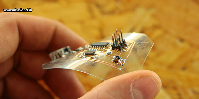
What is a flexible PCB, you may ask. Just as the name suggests, it is a PCB that is not rigid, but flexible in nature. The flexibility comes with the usage of a malleable base material, which holds the circuitry and components on top, just like a normal PCB. The materials used could be polyimide or polyester, with a very thin layer of copper over the board. But, this copper has a tendency to oxidize, which is why the copper layer is covered with another protective layer, such as solder, which has excellent electrical conductivity and zero corrosion capabilities. There are two types of soldering processes that can be followed – manual and laser. Manual soldering is one of the cheapest processes used for welding a PCB, while laser soldering is a faster method. Laser soldering uses the excitation of laser energy to transform into heat energy for soldering.

Advantages of flexible PCBs

Flexible PCBs are easy to install – With the market being filled with nanoelectronics, there is a very small space available to fit the PCBs.  Adjusting the PCB to set into such a compact space can be a challenge. Flexible PCBs male the task much easier.

Flexible PCBs reduce weight and volume – Because flexible PCBs are thin and light in weight, they can also reduce the volume and weight of electronic products, while offering flexibility of installation and excellent electrical properties.

Flexible PCBs offer low risks and high performance – Flexible PCBs reduce the interconnection required, which means lesser solder joints and contact creases. Due to this, potential failures are minimized and performance is improved.

Applications of flexible PCBs

Smartphones – The usage of flexible PCBs is highly increasing, especially in the smartphone industry. Flexible PCB manufacturers are contributing in the industry on a massive level! The demand of flexible PCBs has increased because of the demand of complex circuitries to be installed in the thinnest possible applications.

Wearables – Flexible PCBs have also found great demand in the industry of wearables. That’s because such smartwatches, fitness trackers, and every other kind of sensor-technology device needs to be worn on different parts of the body, which means flexibility is highly required to wrap body parts.

Heads-up displays – Another application is the Heads-up Display used in aerospace, which display operational data directly in the pilot’s field of vision, so that he can read critical operational data during flight, without having to look away from a potential target.

Hearing-assist devices – The medical industry also uses flexible PCBs in hearing-assist devices to provide higher range and resolution than traditional hearing devices, with the usage of flexible PCBs to help mount all the microphone, DSP, and battery in a tiny compact package that fits behind the ear.

To conclude, whenever you are looking for compact, thin, lightweight, flexible, reliable, and efficient PCBs, you know that you are looking for a flexible PCB assembly from India. Get in touch with Miracle Electronics and get your flexible PCBs designed and manufactured as per your requirements. Choose from single-layered, double-layered, and multi-layered options, and have your PCBs designed just the way you want them to be!


Tuesday, 1 December 2020

Building An Efficient PCB Layout - Miracle Electronics

 It is always wise to build PCB prototypes before the entire batch, no matter how big or small the volume of PCBs in a single lot. That’s because a PCB prototype will bring into focus how the PCB will exactly look like and how it will perform. Any faults detected in the prototype can be dealt with before manufacturing a complete batch, so as to avoid an entire lot of PCBs from being made useless, or requiring fixes.

But, the success of failure of a prototype highly depends upon how the PCB has been designed in the first place. Even before the prototyping phase, comes a phase where the designers design a PCB depending upon the requirements and configurations, and plan a layout, on which the engineers work to build a prototype. Any neglections or misinterpretations in the PCB layout can lead to wrongly built or erroneous PCB builds; which is something you certainly don’t want to encounter.

To be able to come up with an efficient PCB layout with no confusions or misunderstandings, there are certain points that need to be considered well; some of them being mentioned below.

Copper traces

It is the copper track that connects two points within the PCB. But, this conductive path can also have resistance. Generally, designers use the length, width, and thickness to control the resistance of the trace, and form the different levels of thickness of a PCB. But, it is always better to use a PCB trace width calculator to determine the optimal thickness for your project. Also, it should be kept in mind that traces on the external layers will cool off better and quicker, while heat from the internal layers are required to travel through the layers of copper, before being conducted. This is the reason why single layered PCBs are most preferred in simpler applications where they can be effectively used.

Distance between copper traces and fills

There must be enough room between the copper traces and fills to prevent any shock hazards. Solder marks aren’t always reliable conductors, which is why a good amount of distance between the two is judicious.

Distance between noise and analog traces

Placing both noise traces and analog traces together will certainly double the signals on the traces, which further leads to interference and short-circuiting. Thus, it is always wise to keep both these high frequency traces away from one another.

Placement of decoupling capacitors

Decoupling capacitors must be placed as near as possible to the power and ground pins of integrated circuits to increase efficiency. Capacitors placed farther away will have a reduced inductance ability.

Loop size

Loops within a PCB design should always be kept as small as possible. That’s because smaller loops have lower inductance and resistance. In addition, a PCB with high loops reduces the amount of high frequency voltage spikes.

With all these tips followed, one can come up with a reliable and efficient PCB layout. If you are in search of one such layout that can help you get the best possible PCB for your application, you can get in touch with Miracle Electronics, where you’ll not only get talented designers working to come up with the most efficient PCB layout, but also expert engineers to help you build a reliable PCB assembly from India. You can rely on Miracle Electronics for all kinds of high volume, medium sized, or even low volume projects, no matter what your industry and application.


Friday, 13 November 2020

How Are Copper Wire Cables Tested - Miracle Electronics

Copper wire cables are a very small part of any electronic application, but that doesn’t mean they are insignificant. In fact, they are one of the most important parts of a circuit that connects different parts and sends power or signals to them for an effective functioning. And, this is why it is highly crucial that these wires and cables are of the best quality. For this, one, you need reliable and experienced wire harness manufacturers from India, who make only genuine high-quality wires with no compromise; and two, you need thoroughly tested wire cables that ensure zero faults. Although a genuine manufacturer will himself test every product before delivering it to you, yet we put it up as a different point to bring to your notice the importance of testing.


Tests done by the manufacturer

There are a variety of different tests that are done on copper wire cables to ensure best quality and perfect functionality.

Continuity test – This test allows to check for solid wire connections within the cable. Multimeters are used to check this by measuring the current, voltage, and resistance of the circuit.

Resistance test – This test helps measure the voltage and current resistance within a cable, which can then be compared to the expected cable performance to reveal how well the cable is performing. An ohmmeter is used for this purpose, where it passes a small current through the cable and measures the voltage drop.

Isolation test – This test uses low voltage power to help see how well isolated the wires within the cable are. A megohmmeter is used to measure current leakage with a low voltage.

Shorts test – This test uses high voltage power to help find any shorts within the cable, which is not revealed when low voltage is used.

Miracle Electronics tops the list of wire harness manufacturers from India, who makes sure to conduct all the above tests and more to ensure high quality and high-performance wires and cables before delivering the same to clients.

Three tests after purchase

While your manufacturer should have done all the above-mentioned tests already, there are three other critical tests that should be done after the purchase. One is to be done during the installation, second during having it to perform the first time, and third is during frequent maintenance procedures.

During installation – You must check for any damage during transit, and ensure that the cables are working, upon installation.

When functioning first time – Once you install the cables, turn on your application and thoroughly check for any interference or problems. The cables must be compatible, and must seamlessly interact with the software and other elements involved with the application.

Frequent maintenance procedures – You must carry out maintenance procedures periodically to check if the integrity of the cables have been compromised after a set period of time, or following peak load times.

With all the above tests, you can ensure quality performance and safe procedures within the space where the application has been installed.


Wednesday, 21 October 2020

Cables And Wires For Medical Applications - Miracle Electronics

When looking to satisfy medical applications, you need a perfect manufacturer  that has a great experience of manufacturing cables and wires for such sensitive products. They must have a thorough understanding of the particularly rigorous standards and regulations that apply to the medical industry. After all, you’ll need only the highest quality cables and wires in the market, suitable for all kinds of medical applications like diagnostic equipment, laboratory equipment, treatment equipment, lighting systems, automation devices, and more.


Diagnostic equipment

Medical diagnostic equipment and imaging equipment like MRIs, PET scans, CT scans, X-rays, and ultrasounds are critical for the diagnosis and treatment of patient injuries and ailments. And, all such critical equipment requires high-performance and reliable wiring connections so that information can be transferred accurately and in a secured manner.

Laboratory equipment

Laboratory equipment like life support equipment, dialysis machines, ventilators, anesthetic dispensers, and more require cables that can ensure accurate measurement, monitoring, and analysis of patient health. These equipment are highly sensitive and critical, used to help medical professionals examine body fluids for signs of disease or infection.

Treatment equipment

There are a variety of tools that are used in the medical industry for treating a variety of health problems; for instance, surgical lasers, medical infusion pumps, and LASIK equipment, to name a few. All these equipment, as well as the operating tables must be equipped with reliable cables and wires to ensure appropriate positioning of the patient during sensitive procedures.

Lighting systems

When any kind of treatment is being executed, may it be a simple LASIK operation, or a significant heart operation, nothing can be executed successfully without the use of extremely bright lighting. And, for such bright lighting, it is important that extremely reliable and durable wires and cables are used that can withstand high power levels, and also extreme temperature fluctuations.

Automation devices

Automation is becoming more common in medical practice today to provide medical practitioners with accurate, quick, and efficient procedures. But, to be able to make the automation precise and reliable, data cables that receive and transmit instructions, and also sensor cables that transmit critical information to the operating system in real time, need to be efficient as well as have the ability to withstand all kinds of bends, turns, and other motions.

These are just some of the medical applications that use wires and cables of various types. There is so much more than the healthcare industry calls for. But, no matter what the application or requirement, every medical equipment and process requires efficient, high-performing, durable, and reliable connections. You thus need high quality cables and wires; and for that to be possible, you need experienced and trustworthy wire and cable manufacturers. Miracle Electronics is one of the best cable and wire harnessmanufacturers from India, where you can get not only all of the above, but also customized engineered solutions, tailored to meet your particular needs at the premises that is designed to create cable and wire products that meet the most stringent industry standards.


Friday, 16 October 2020

Copper Wires _ Benefits & Applications - Miracle Electronics

 Copper is a very common metal used in all kinds of electrical applications, because it is considered as one of the best materials for conducting electricity. Today, the material is used in electrical wiring for both domestic and industrial use in a variety of applications like electronic circuitry, home appliances, telecommunications, etc. In fact, half of all the copper that is mined today is used to produce wires and cable conductors! Copper is thus a versatile metal of the future.


What makes copper so popular and admired?

Copper possesses excellent electrical and thermal conductivity

Copper has the best know electrical and thermal conductivity, better than any other conducting metal. It has the least resistance to conduction, hence it can be used in even the highest conductivity applications like lightning rods for safety measures in buildings and skyscrapers.

Copper has great tensile strength

Copper has excellent tensile strength and can also resist a number of mechanical failures like stretching, breaking, necking, etc; thus achieving so much of admiration.

Copper is highly malleable and ductile

Copper is a very highly malleable and ductile metal, which makes it very easy to draw it into wires, strips, and strands. This is why copper finds so much admiration in the applications of wiring.

Copper can be easily soldered

Copper wires can be easily soldered to form connections, making connections easy for transmission and termination points. Moreover, the excellent strength that copper possesses makes it possible to pull it through different areas, and even tiny tight spaces to lay conduits.

Copper has good corrosion resistance

Copper’s great corrosion resistance makes it one of the best metals to be used for electrical transmission. Its low reactivity series does not let it corrode, thus making it an excellent choice to be used in wires.

Copper has excellent creep resistance

When a metal expands and contracts under certain cyclic load conditions, the deformation that results is known as creep. When there’s higher creep, a screw can deform a conductor and reduce contact pressure, which leads to resistance in joints, loose connections, oxidation, and overheating. But, copper has an almost negligible creep, making it the best metal to be used in a wire.

Types of copper wires

With the amazing properties that copper possesses, it now becomes clear why the metal is so popularly used in wires and cables. But, did you know that there are a variety of different copper wires available for you to choose from?

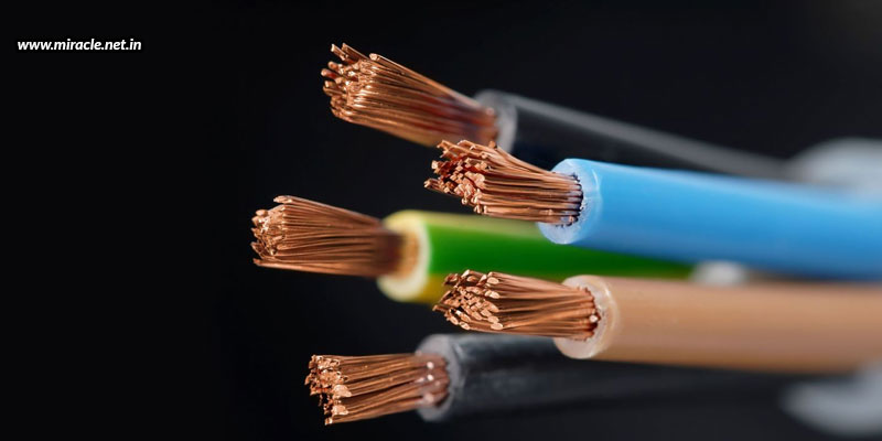
Solid copper wire – This is a single copper wire, bare or sheathed , in an insulating cover, used to transfer electricity.

Stranded copper wire – This is when numerous thin copper wires are wound together to form a single wire.

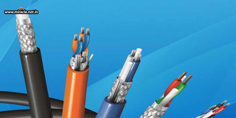
Copper cable – When copper wires are twisted, braided, twisted, or woven into a single assembly, a copper cable is produced.

We’ve learnt all about copper wires and cables, and how they are such a great choice. But, it is essential that you rely on a genuine copper wire manufacturer to ensure that you get good quality and unadulterated copper wires that are proven and certified. And, MiracleElectronics tops the list of the most reliable and trustworthy wire harness manufacturers from India, where you can get all kinds of wires and wire harness, customized to your specific needs, each being high on quality and certified for production processes.

Thursday, 10 September 2020

Why Should Industrial Bus Cables Be Standardized - Miracle Electronics

The two main sectors for series data cables are computer bus and industrial bus; the former being a communication system that transfers data between components inside or between computers; and the latter being a communication system that transfers data between components or devices at different levels in a manufacturing plant. But, it is the computer industry that has had greater success in achieving unbiased industry-wide standards, while the industrial sector is more independent, and can produce cables specifically for their brand names.

In the industrial world, there are a number of variations due to different speed and impedance requirements, ranging from 100 to 150 ohms. Moreover, manufacturers may design a hybrid cable for automotive manufacturing plants with components using PROFINET, INTERBUS, and Industrial Ethernet protocols, all in one cable; allowing them to connect their PLC logic to whatever control line happens to come on the next machine.

Protocol standardization

Industries are looking for open architecture interface as the need for plant-wide system compatibility increases. Ethernet protocol of 100 ohms seems to be a good choice in this case. Higher information speed requirements, diagnostic feedback of controls, and interest in motor feedback make Ethernet a great choice to offer the performance required. However, these requirements are still driven from the controls manufacturers’ system trademark, some of them being PROFINET, CC-Link IE, Industrial Ethernet, and Foundation Fieldbus HP. Yet, many independent special interest groups have started to come up and work for system compatibility of conventional Ethernet. One such example is Ethernet POWERLINK Standardization Group that has developed a formidable product offering with data transmission speeds of 100 Mbit/sec; and is waiting for component manufacturers to adopt their standard Ethernet protocol into their systems.

Connector standardization

The standardization of connectors is also being accepted as major device dealers are settling for metric-type connectors like M-8, M-10, and M-12. RJ45 is also used, but it is modified to provide larger gauge compatibility, harsh environment resistance, and shielding capabilities.

To conclude

As you can see, Ethernet-based architecture is becoming an accepted choice for serial bus networks, since the compatibility and standardization of Ethernet from the computer side, found in front office, drives the manufacturing side to generic products. However, the marketing side of the controls industry still continues to manufacture proprietary products, developing cable requirements that are exclusive to the brand. Having such a diversity of protocols allows cable manufacturers to offer a lot many different cable systems. Also, each architecture has a unique conductor configuration and electrical requirements.

From past to present

The goal of various bus protocols and designs developed over the last 50 years was to find a cable capable of fast computer speeds that could withstand electrical noise and harsh environments. To accomplish this goal, technology is advancing to produce fiber optic cables, which is more suited to these requirements.

Whatever kind of cables you’re looking for – basic or fiber optic – Miracle Electronics is where you should be. These are the most dependable and versatile wire harness manufacturers from India, manufacturing a variety of different types of cables and harnesses for a myriad of applications and industries. You can also get in touch to design the perfect customized cable harness for your requirements.


Monday, 7 September 2020

HDI PCBs _ Why And Where To Use Them - Miracle Electronics

As we’re all shifting more and more to studying, working, browsing, and shopping online, after the pandemic has struck us, our world is becoming even more dependent on digital technologies. Moreover, the digital world today is becoming even more complex; but the hardware associated with it is becoming smaller. For instance, PCBs are becoming smaller with more interconnections. This makes the applications they are used in sleek and lean. And, if they are portable, it becomes really convenient to carry the devices around.


The PCB industry plays a significant role in the development of all electronic gadgets that our lives revolve around today. And, to make it simpler and easier, PCB manufacturers are always coming up with newer trends; one such innovation being the HDI PCB, which is a smaller PCB assembly from India that is dense with high component count.

What is HDI PCB?

HDI PCBs are smaller PCBs with a high density component count, and thus more number of interconnections, but those that occupy lesser space. Although the components are placed very close to one another to reduce the size of the board, the functionality isn't compromised. The general HDI PCB is one that has an average of 120 to 160 pins per square inch, and a dense circuitry that is implemented through microvias, buried vias, and blind vias.

What are the advantages of HDI PCBs?

HDI PCBs offer many advantages over regular PCBs, some of them being a compact design, lighter weight, and great performance. In addition, the signal path length is reduced as the components are placed very close to one another, and the reflections of signal are reduced, which results in remarkably improved signal quality. Also, the implementation of stacked vias makes these boards a super shield against extreme environmental conditions. All in all, with so many advantages offered, HDI PCBs are extremely cost-effective.

What are the applications of HDI PCBs?

HDI PCBs, because of the benefits they offer, are used in a variety of industries, such as those listed below.

Smartphone industry – With smartphones becoming more of a necessity than a luxury, manufacturers are using HDI PCBs to make these phones even smaller, and thus, conveniently portable.

Automotive industry – Car manufacturers are using more of HDI PCBs to save significant space in the vehicles. Moreover, the integration of smaller and smarter electronic devices provides a better driving experience.

Medical industry – Medical devices manufactured today use more of HDI PCBs when they want to fit into small compact devices like implants, lab equipment, and imaging equipment. In diagnostic devices, miniaturized cameras using HDI PCBs can help get better and intricate picture quality.

Aerospace and military industries – Aerospace and military equipment like planes, missiles, and defense systems use HDI PCBs that can function better in extreme environments and hazardous conditions.

Wearable technology industry – Wearable devices like VR headsets, watches, and many others use HDI PCBs to make the devices sleek, while offering exceptional functionality.

You can see how HDI PCBs have revolutionized almost every industry today with usage in a variety of devices and applications. This has increased the demand for such PCBs. You may also opt for such advanced and improved PCBs to fit into your smaller and smarter products. You can choose from readily available PCBs or have your PCB assembly from India especially customized as per your requirements at Miracle Electronics, the leader in manufacturing a variety of PCB assemblies since more than a decade now.


Tuesday, 19 May 2020

Factors To Consider While Manufacturing A Switch Gear - Miracle Electronics

Electric power has become a basic necessity for each one of us today; and for electric power circuits to operate well, it is important that they are operated by the right switch gear controls, which can switch and protect individual components of the equipment. Composed of electrical disconnect switches, fuses, and circuit breakers to control, protect, and isolate electrical equipment, switch gears are used to de-energize equipment so hat work can be performed with zero faults down the line.

These equipment are thus directly linked to the reliability of the electric supply; and must be thus manufactured very cautiously. So, when you are looking to manufacture such important components for your application, it is crucial that you consider several factors so as to develop and implement these components properly.
The size of the switch gear
The first and foremost consideration is the size of your switch gear. What size of switch gear will be apt for your application? Especially, when maintenance is concerned, you need to have an appropriate switch gear, if you need to move it in and out of the enclosure at the base for repairs and upkeep.
The environmental factors it will encounter
Where are you planning to install your switch gear? What is the application? Where will your product be used or installed? What kind of environmental factors will the switch gear encounter? For example, if the environmental conditions are of extreme temperatures or humidity, you need to design your switch gear such that they can effectively perform under those circumstances.
The operation requirements
You also need to consider the general control action of the switch gear. Are there any special requirements you need your switch gear to perform? Whatever your requirements, you need to present the information to the manufacturer right at the beginning of the development phase. Depending upon all that you require from your switch gear, the design plans will be worked out; and based on the finalized plan, the manufacturing will be carried out. Hence, every tiny information should be communicated and clarified before moving into the manufacturing phase to ensure that every specification of the switch gear will complement your equipment operation requirements.
Typically, switch gear are located on both high and low voltage sides of large power transformers. The switch gear on the low voltage side of transformers may be located in a building, with medium voltage circuit breakers for distribution circuits, along with control, protection, and metering equipment. For industrial applications, transformers and switch gear are combined into one housing, known as a unitized substation. So, for any queries on switch gear and transformers, and their components, or to place an order, you can always get in touch with Miracle Electronics, the best transformer manufacturer in India , where you can communicate all your information with skilled technicians, and have only the best electronic components manufactured for you. You can have almost every kind of electronics manufacturing services offered here, right from product and system designing to manufacturing the best quality products.